
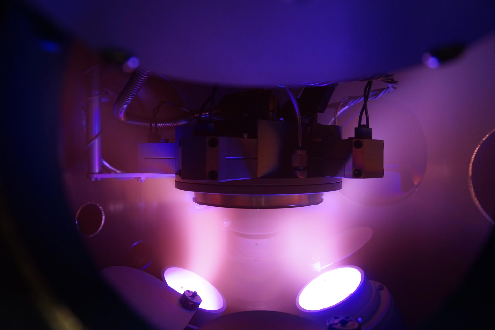
In the clean, silent depths of a vacuum chamber, a storm is raging—one that could tear up the foundations of microchip manufacturing as we know it.
It’s called the “electron shower,” and it’s the secret weapon behind a new technology that’s finally cracked a problem that has held back next-gen electronics for decades: how to build ultra-thin, ultra-precise films on delicate insulating surfaces without frying them—or embedding microscopic landmines in the form of unwanted particles.
At the center of this breakthrough is a clever upgrade to a powerful method known as HiPIMS (High Power Impulse Magnetron Sputtering). Sounds like sci-fi—and in many ways, it is. This technique uses short, brutal pulses of energy to blast atoms off a target and shoot them toward a surface, forming films that are harder, purer, and better structured than those made by traditional means.
But HiPIMS has had a fatal flaw: too much argon. The very plasma that enables it also floods the process with stray argon ions, which, if embedded in the film, can sabotage delicate electronic components—especially piezoelectric films, the whisper-thin layers that let your phone hear you, your car detect collisions, and your smartwatch track your heartbeat.
Enter timing. Empa researchers in Switzerland figured out that the plasma soup doesn’t all arrive at once. Argon ions get there first. If you zap the target with a voltage spike after they’ve passed, you only accelerate the good stuff—the target atoms you actually want in your film.
But that was just the beginning.
To coat insulating materials like glass or sapphire—essential in chips, quantum devices, and future sensors—the team needed something even more exotic. Their solution? Use the chamber’s own electron fallout as a weapon. Every plasma pulse sends a burst of negatively charged electrons to the surface. These aren’t just background noise—they’re fuel. If triggered precisely, these microbursts can create just enough charge to pull in the right ions, skipping the argon and delivering atomic perfection.
This synchronized trick, dubbed SFP-HiPIMS, allows for flawless piezoelectric film creation on surfaces that were previously off-limits—and at temperatures low enough for advanced chip manufacturing.
What does this mean? We’re not just talking about a better way to make filters for your smartphone. This is about building the thin-film infrastructure for quantum computing, photonic chips, and neural implants. It’s a pathway to an electronics world that’s faster, more flexible, and radically more precise.
The Empa team isn’t stopping here. With machine learning, high-throughput testing, and a swarm of collaborations already underway, they’re turning this one-time laboratory trick into a scalable process that could redefine how we build the next era of electronics.
The revolution isn’t loud. It’s an invisible storm of electrons—synchronized, weaponized, and rewriting the atomic rules of the game.