
At Tianjin University, scientists have developed a revolutionary method to test micro-LED wafers without causing damage—solving a key obstacle that has long hindered the high-end display industry. Using just 0.9 megapascals of pressure, the team has introduced a soft-contact approach that offers a viable path to scaling up production of ultra-bright, energy-efficient screens for everything from luxury televisions to next-generation wearables.
Micro-LED technology holds immense promise, but commercial success hinges on achieving exceptionally high yields during wafer fabrication. Even minor defects in these tiny LED structures can degrade performance, increase costs, and delay production. As a result, rigorous quality testing is essential—but testing itself has been a persistent problem.
Traditional probe-based inspection methods often risk scratching or damaging the wafer surface. Meanwhile, non-contact methods like optical or infrared imaging can miss fine defects, limiting their effectiveness. This bottleneck has made it difficult to scale micro-LED production efficiently.
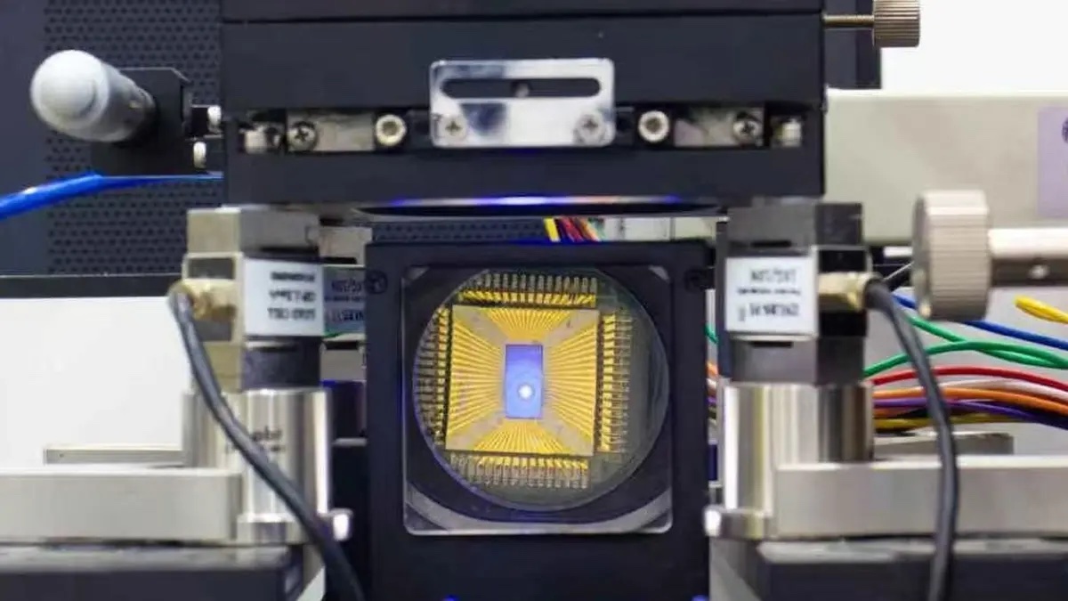
Now, a research team led by Professor Huang Xian from the School of Precision Instrument and Opto-electronics Engineering has introduced a solution: a non-destructive testing system that uses a flexible 3D probe array. The system gently adapts to the wafer’s microscopic surface and applies a pressure as low as 0.9 MPa—about as soft as a breath of air.
The probes exert just one ten-thousandth the pressure of conventional rigid probes, preserving the delicate wafer surface and significantly extending the lifespan of the testing equipment. Even after one million test cycles, the probes remain in excellent condition.
Complementing this soft-contact system is a custom-built measurement platform that integrates seamlessly with the flexible probes. Together, the system supports high-throughput electrical testing—crucial for verifying wafer quality in mass production environments.
The timing of this breakthrough is critical. As companies race to commercialize micro-LED displays, the demand for scalable, low-cost, and damage-free testing solutions is surging.
According to Professor Huang, this advancement fills a major technical gap in micro-LED electroluminescence testing and lays the foundation for broader applications, including advanced wafer inspection and biophotonics. Commercialization of the technology is already underway at the Tiankai Higher Education Innovation Park in Tianjin.
If successfully scaled, this innovation could not only accelerate the growth of the micro-LED industry but also open new frontiers in flexible electronics, sensors, and even medical devices.
By Impact Lab
